Intro
Intro#
SKiDL is a module that allows you to compactly describe the interconnection of electronic circuits and components using Python. The resulting Python program performs electrical rules checking for common mistakes and outputs a netlist that serves as input to a PCB layout tool.
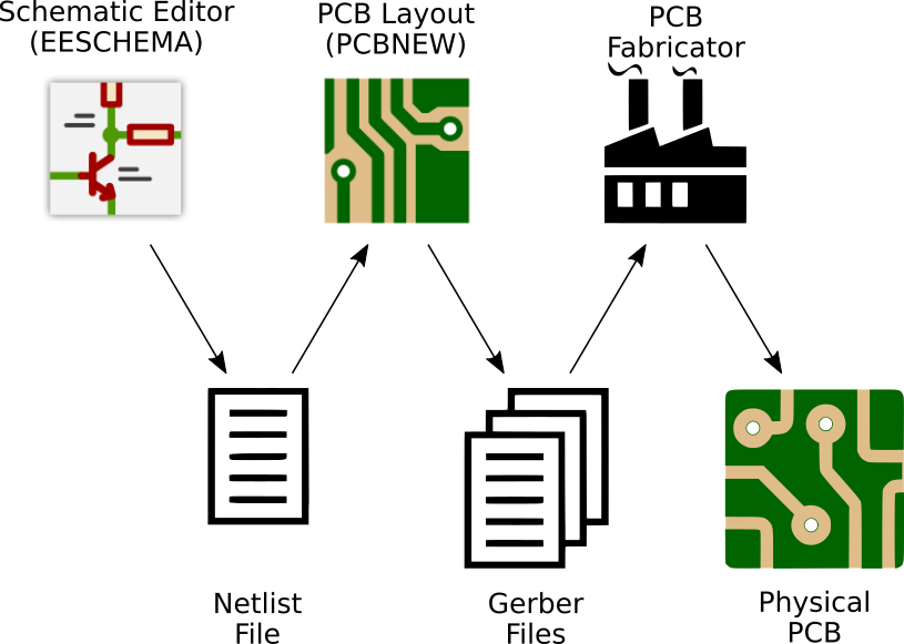
First, let’s look at a “normal” design flow in KiCad:

Here, you start off in a schematic editor (for KiCad, that’s EESCHEMA) and draw a schematic. From that, EESCHEMA generates a netlist file that lists what components are used and how their pins are interconnected. Then you’ll use a PCB layout tool (like KiCad’s PCBNEW) to arrange the part footprints and draw the wire traces that connect the pins as specified in the netlist. Once that is done, PCBNEW outputs a set of Gerber files that are sent to a PCB fabricator who will create a physical PCB and ship it to you. Then you’ll post a picture of them on Twitter and promptly dump them in a drawer for a few years because you got bored with the project.
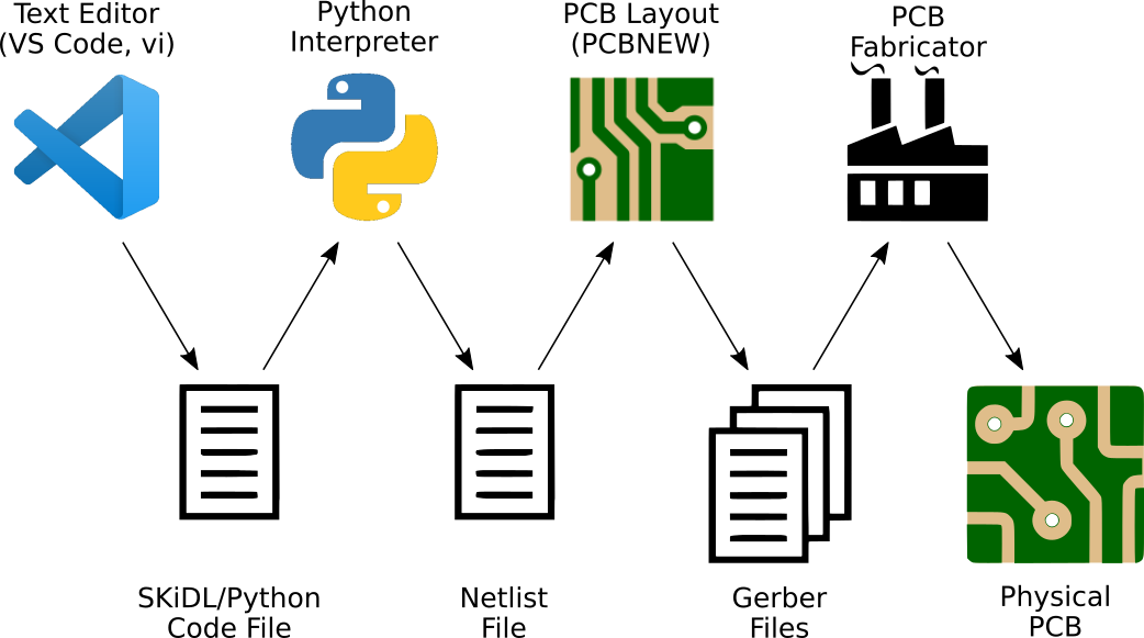
In the SKiDL-based design flow, you use a text editor to create a Python code file that employs the SKiDL library to describe interconnections of components. This code file is executed by a Python interpreter and a netlist file is output. From there, the design flow is identical to the schematic-based one (including dumping the PCBs in a drawer).

So, why would you want to use SKiDL? Here are some of the features SKiDL brings to electronic design:
Requires only a text editor and Python.
Has a powerful, flexible syntax (because it is Python).
Permits compact descriptions of electronic circuits (think about not tracing signals through a multi-page schematic).
Allows textual descriptions of electronic circuits (think about using diff and git for circuits).
Performs electrical rules checking (ERC) for common mistakes (e.g., unconnected device I/O pins).
Supports linear / hierarchical / mixed descriptions of electronic designs.
Fosters design reuse (think about using PyPi and Github to distribute electronic designs).
Makes possible the creation of smart circuit modules whose behavior / structure are changed parametrically (think about filters whose component values are automatically adjusted based on your desired cutoff frequency).
Can work with any ECAD tool (only two methods are needed: one for reading the part libraries and another for outputing the correct netlist format).
Takes advantage of all the benefits of the Python ecosystem (because it is Python).
Free software: MIT license.
Open source: https://github.com/devbisme/skidl
As a very simple example, the SKiDL program below describes a circuit that takes an input voltage, divides it by three, and outputs it:
from skidl import *

# Create input & output voltages and ground reference.
vin, vout, gnd = Net('VI'), Net('VO'), Net('GND')

# Create two resistors.
r1, r2 = 2 * Part("Device", 'R', TEMPLATE, footprint='Resistor_SMD.pretty:R_0805_2012Metric')
r1.value = '1K'   # Set upper resistor value.
r2.value = '500'  # Set lower resistor value.

# Connect the nets and resistors.
vin += r1[1]      # Connect the input to the upper resistor.
gnd += r2[2]      # Connect the lower resistor to ground.
vout += r1[2], r2[1] # Output comes from the connection of the two resistors.

# Or you could do it with a single line of code:
# vin && r1 && vout && r2 && gnd

# Output the netlist to a file.
generate_netlist()
And this is the netlist output that is passed to PCBNEW to do the PCB layout:
(export (version D)
  (design
    (source "/media/devb/Main/devbisme/KiCad/tools/skidl/skidl/circuit.py")
    (date "04/21/2021 10:43 AM")
    (tool "SKiDL (0.0.31)"))
  (components
    (comp (ref R1)
      (value 1K)
      (footprint Resistor_SMD.pretty:R_0805_2012Metric)
      (fields
        (field (name F0) R)
        (field (name F1) R))
      (libsource (lib Device) (part R))
      (sheetpath (names /top/15380172755090775681) (tstamps /top/15380172755090775681)))
    (comp (ref R2)
      (value 500)
      (footprint Resistor_SMD.pretty:R_0805_2012Metric)
      (fields
        (field (name F0) R)
        (field (name F1) R))
      (libsource (lib Device) (part R))
      (sheetpath (names /top/3019747424092552385) (tstamps /top/3019747424092552385))))
  (nets
    (net (code 1) (name GND)
      (node (ref R2) (pin 2)))
    (net (code 2) (name VI)
      (node (ref R1) (pin 1)))
    (net (code 3) (name VO)
      (node (ref R1) (pin 2))
      (node (ref R2) (pin 1))))
)
